Every electronic device you use — your smartphone, your laptop, your microwave, your car’s navigation system — has at least one printed circuit board inside it. That board is the result of two closely related but distinct manufacturing processes: PCB fabrication and assembly. Together, these two processes transform a digital design into a fully functional electronic board ready to power the devices we rely on every day.
In this article, we’ll break down what PCB fabrication and assembly each involve, how they differ, how they work together, and what you need to know if you’re looking to manufacture your own circuit boards.
Understanding the Difference: Fabrication vs. Assembly
Before diving into the details, it’s important to understand the distinction between the two processes:
PCB Fabrication is the process of manufacturing the bare circuit board itself — the physical substrate with copper traces, drilled holes, and surface finishes, but without any electronic components on it. Think of it as building the foundation of a house before any furniture goes in.
PCB Assembly is the process of populating that bare board with electronic components — resistors, capacitors, microchips, connectors, and more — and soldering them in place to create a fully functional electronic circuit. This is like furnishing and fitting out the house so people can actually live in it.
Both processes are essential, and the quality of each directly affects the performance and reliability of the finished product. A beautifully assembled board built on a poorly fabricated substrate will still fail. Equally, a perfectly fabricated board assembled carelessly will produce defective electronics. The two must work together seamlessly.
Part One: PCB Fabrication
PCB fabrication is a multi-step manufacturing process that begins with a digital design file and ends with a physical bare board. Here’s how it works:
Step 1: Design and File Preparation Everything starts with the PCB design, created using Electronic Design Automation (EDA) software such as Altium Designer, KiCad, or Eagle. The finished design is exported as a set of Gerber files — the industry-standard format that describes each layer of the board, including copper traces, solder mask, silkscreen, and drill locations.
Before fabrication begins, these files go through a Design Rule Check (DRC) and a Design for Manufacturability (DFM) review to catch any errors or issues that could cause problems during manufacturing.
Step 2: Substrate Preparation The base material of most PCBs is FR4 — a fiberglass-reinforced epoxy laminate coated with a thin layer of copper on one or both sides. The substrate is cut to the required panel size and cleaned before processing begins.
Step 3: Inner Layer Imaging (for Multi-Layer Boards) For multi-layer PCBs, the inner copper layers are processed first. A photosensitive film called photoresist is applied to the copper-clad substrate. The board is then exposed to UV light through a photomask that represents the copper pattern for that layer. The exposed areas harden, while the unexposed areas are washed away, leaving the desired copper pattern behind.
Step 4: Etching The board is immersed in a chemical etching solution — typically ferric chloride or ammonium persulfate — that dissolves the exposed copper areas not protected by the hardened photoresist. What remains is the precise copper trace pattern defined in the design.
Step 5: Layer Lamination For multi-layer boards, the individual inner layers are stacked and laminated together under heat and pressure, with prepreg (a partially cured fiberglass material) between each layer acting as an insulating adhesive. This creates a solid, unified multi-layer board.
Step 6: Drilling Holes are drilled through the board at precise locations — for through-hole component leads, vias (connections between layers), and mounting points. Modern PCB fabrication uses computer-controlled drilling machines capable of creating holes as small as 0.1mm with exceptional accuracy.
Step 7: Plating To make the drilled holes electrically conductive (so signals can pass between layers), the inside of each hole is coated with a thin layer of copper through an electroplating process. This is one of the most technically demanding steps in PCB fabrication.
Step 8: Outer Layer Imaging and Etching The same imaging and etching process used for inner layers is applied to the outer copper layers, defining the final copper pattern on the top and bottom of the board.
Step 9: Solder Mask Application A protective coating called solder mask — typically green, though other colors like blue, red, and black are also common — is applied over the copper traces. This coating insulates the traces, protects them from oxidation, and prevents solder bridges during assembly. The solder mask is applied everywhere except on the solder pads where components will be attached.
Step 10: Surface Finish The exposed copper pads are coated with a surface finish to prevent oxidation and ensure good solderability. Common surface finishes include HASL (Hot Air Solder Leveling), ENIG (Electroless Nickel Immersion Gold), OSP (Organic Solderability Preservative), and ENEPIG (Electroless Nickel Electroless Palladium Immersion Gold).
Step 11: Silkscreen Printing Reference designators, component outlines, logos, and other markings are printed onto the board’s surface using a silkscreen process. This helps assemblers identify where each component goes and makes troubleshooting easier down the line.
Step 12: Electrical Testing and Inspection Before leaving the fabrication facility, bare boards are tested using a flying probe or bed-of-nails tester to verify that all electrical connections are correct and there are no shorts or open circuits. Automated Optical Inspection (AOI) may also be used to verify dimensional accuracy and trace integrity.
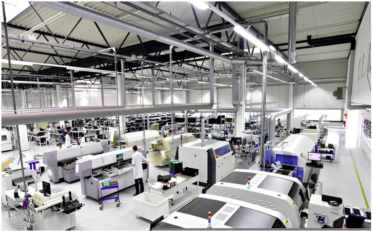
Part Two: PCB Assembly
With the bare board fabricated and verified, it moves on to the assembly stage — where it comes to life. PCB assembly involves placing and soldering electronic components onto the board, following the design’s Bill of Materials (BOM) and assembly drawings.
Surface Mount Technology (SMT) Assembly The majority of modern PCB assembly uses Surface Mount Technology, where compact SMD (Surface Mount Device) components are placed directly onto the board’s surface. The SMT assembly process involves:
- Solder paste printing: Solder paste is applied to the component pads through a metal stencil
- Pick-and-place: Automated machines place each component onto the solder paste with high precision
- Reflow soldering: The board passes through a reflow oven, melting the solder paste and forming permanent electrical connections
Through-Hole Assembly Some components — particularly large connectors, transformers, and electrolytic capacitors — are still available in through-hole form and require a different assembly approach. Their leads are inserted through holes in the board and soldered on the underside, either manually or using wave soldering equipment.
Mixed Technology Assembly Many modern PCBs use both SMT and through-hole components, requiring a combination of both assembly methods. The SMT components are typically assembled first, followed by the through-hole components.
Inspection and Quality Control After soldering, assembled boards go through rigorous inspection and testing:
- Automated Optical Inspection (AOI) checks for missing, misaligned, or incorrectly soldered components
- X-ray inspection examines hidden solder joints beneath BGA packages
- In-Circuit Testing (ICT) verifies individual component values and connections
- Functional testing confirms the board performs correctly under real operating conditions
Why PCB Fabrication and Assembly Quality Matter
The quality of PCB fabrication and assembly directly determines the reliability and performance of the finished electronic product. Poor-quality fabrication can result in trace delamination, via failures, or impedance issues that compromise signal integrity. Substandard assembly can produce cold solder joints, solder bridges, or misplaced components that cause intermittent failures or complete non-function.
For consumer electronics, quality issues mean product returns and damaged brand reputation. For medical, automotive, or aerospace applications, they can have far more serious consequences. This is why reputable manufacturers invest heavily in process controls, quality management systems, and testing infrastructure — and why choosing the right manufacturing partner is so important.
What to Look for in a PCB Fabrication and Assembly Partner
Whether you’re producing a prototype or scaling to full production, choosing the right manufacturing partner can make or break your project. Here’s what to look for:
Integrated Services: Providers that offer both fabrication and assembly under one roof streamline communication, reduce lead times, and minimize the risk of errors during the handoff between processes.
Certifications: Look for ISO 9001 quality management certification, IPC-A-600 for bare board quality, and IPC-A-610 for assembly quality. Industry-specific certifications such as AS9100 (aerospace) or ISO 13485 (medical) may also be relevant.
Engineering Support: A good partner provides DFM feedback, design reviews, and technical guidance to help you avoid costly mistakes before production begins.
Transparency: Clear pricing, realistic lead times, and open communication about potential issues are hallmarks of a trustworthy manufacturing partner.
Scalability: Choose a partner who can support you from prototype through to full production, so you don’t have to switch manufacturers as your volumes grow.
Conclusion
PCB fabrication and assembly are two sides of the same coin — complementary processes that together transform a design concept into a fully functional electronic board. Understanding how each process works, and how they interact, is essential for anyone involved in electronics development or manufacturing. Whether you’re building your first prototype or scaling up to high-volume production, getting both processes right is critical to the success of your product. For companies seeking a reliable, high-quality manufacturing partner, PCB fabrication and assembly in China offers a compelling combination of technical expertise, advanced manufacturing infrastructure, rigorous quality standards, and competitive pricing — making it one of the most popular choices for electronics manufacturers around the world.